NINE LEVEL INVERTER BASED ON SWITCHED CAPACITOR STRUCTURE
DECLARATION
I hereby declare that the project report ( Nine Level Inverter based on Switched Capacitor Structure), submitted for partial fulfillment of the requirements for the award of degree of Bachelor of Technology of the APJ Abdul Kalam Technological University, Kerala is a bonafide work done by me under supervision of T.G. SANISH KUMAR, Associate Professor, Government Engineering College, Thrissur. This submission represents my ideas in my own words and where ideas or words of others have been included; I have adequately and accurately cited and referenced the original sources. I also declare that I have adhered to ethics of academic honesty and integrity and havenot misrepresented or fabricated any data or idea or fact or source in our submission. I understand that any violation of the above will be a cause for disciplinary action by the institute and/or the University and can also evoke penal action from the sources which have thus not been properly cited or from whom proper permission has not been obtained. This report has not been previously formed the basis for the award of any degree, diploma or similar title of any other University.
ACKNOWLEDGEMENT
During the course of my project work several persons collaborated directly and indirectly with me. Without their support it would be impossible for me to finish my work. That is why I wish to dedicate this section to recognize their support. I want to start expressing my thanks to my project guide T.G Sanish Kumar, Associate Professor Dept. of Electrical Engineering, because of his valuable advice and guidance towards this work. I received motivation; encouragement and hold up from his during the course of work. I am thankful to Dr. Reji P, Head of the Department, and our Principal Dr Sheeba V.S, for their sole co-operation. I am grateful to express my thanks to all the faculty members of our department for their support. I articulate my gratitude to all my associates and colleagues for their support and help for this work. Last, but not the least I wish to express my gratitude to God Almighty for His abundant blessings without which this effort would not have been successful.
ABSTRACT
Multilevel inverter is a power electronic device capable of providing desired output using multiple lower level DC voltages as an input. Multilevel inverters are gaining popularity over conventional two level inverters because it can produce a smoother stepped output waveform. Moreover, the output obtained from multilevel inverters has lower dv=dt and lower harmonic distortions. Multilevel inverters usually make use of diode clamped, flying capacitor or cascaded H-bridge topologies. These topologies suffer from disadvantages
such as multitude of components, large size and cost as well as complex control. This project aims to use a switched-capacitance (SC) structure to overcome the disadvantages of the existing topologies. It involves adding an SC structure to the H-bridge inverter using capacitors, switches and diodes to create a multilevel DC voltage at the DC bus of the H-bridge circuit. The proposed technology will improve upon the existing technology by having boost operation without magnetic elements, fewer components, less complex control and using only one power DC source. This project work involves the simulation and hardware implementation of Nine level Inverter based on Switched Capacitance Structure.
📄 Full Project Report
For complete details about this project, including comprehensive analysis, simulation results, hardware implementation, and testing, please refer to the full project report:
📥 Download Full Project Report (Report.pdf)
PROJECT TEAM
| Name | Roll No |
|---|---|
| ABHILASH M M | TCR15EE002 |
| ALIN ANTO | TCR15EE016 |
| DEVIKA SAJEEV | TCR15EE042 |
| DON DEV | TCR15EE046 |
Department: Electrical and Electronics Engineering
Institution: Government Engineering College, Thrissur
University: APJ Abdul Kalam Technological University, Kerala
Year: May 2019
PROJECT OBJECTIVES
The project aims to design and implement a multilevel inverter that overcomes the disadvantages of existing topologies:
Problems with Current Topologies:
- Large number of components (switches, power supplies, capacitors, and diodes)
- Large size and high cost
- Complex control
Proposed Solutions:
- Fewer components - Switches, sources and capacitors significantly reduced
- Smaller and less expensive - Optimized design reduces overall system cost
- Less complex control - Simplified switching strategy
- Single DC source - Requires only one power supply
- Boost operation without magnetic elements - Achieves voltage multiplication using capacitive elements
SYSTEM REQUIREMENTS
Hardware Requirements
- DSO (Digital Storage Oscilloscope) - Analysis and measurement
- DSP (Digital Signal Processor) - Controller for switching logic
- Function generator - Analysis and reference signal generation
Software Requirements
- MATLAB - Simulation and analysis
- Proteus - Circuit design and simulation
- LaTeX - Documentation
KEY TECHNICAL SPECIFICATIONS
Simulation Specifications
| Parameter | Value |
|---|---|
| Input Voltage (V_in) | 36V |
| Output Voltage (V_out) | 100V |
| Power Rating | 100W |
| Capacitor C1 | 2400 μF, 180V |
| Capacitor C2 | 3600 μF, 180V |
| Load (R+jX) | 100 + j12 Ω |
| Carrier Frequency | 5000 kHz |
| Modulation Frequency | 50 Hz |
| Switching Scheme | Phase Disposition PWM (PDPWM) |
Hardware Specifications
| Component | Specification |
|---|---|
| Switch | MOSFET IRFP460 |
| Diode | MUR460 |
| MOSFET Driver | TLP250 Opto-coupler |
| Controller | DSPIC30F2020 |
| Capacitor C1 | 2400 μF, 180V |
| Capacitor C2 | 3600 μF, 180V |
| Carrier Frequency | 5000 kHz |
| Modulation Frequency | 50 Hz |
| Switching Scheme | PDPWM |
SWITCHED CAPACITOR TOPOLOGY COMPARISON
| Topology | Capacitors | Diodes | Switches | DC Sources |
|---|---|---|---|---|
| Switched Capacitor MLI | 2 | 2 | 9 | 1 |
| Diode Clamped MLI | 8 | 28 | 32 | 1 |
| Flying Capacitor MLI | 64 | 0 | 32 | 1 |
| Cascaded H-Bridge MLI | 0 | 0 | 16 | 4 |
The proposed Switched Capacitor topology significantly reduces the number of components required compared to existing multilevel inverter topologies.
SWITCHED CAPACITOR STRUCTURE
Operating Modes
| Mode | Output Voltage | Configuration |
|---|---|---|
| Mode 1 | V_in | Source and C1 in parallel |
| Mode 2 | 2V_in | Source and C1 in series, then parallel with C2 |
| Mode 3 | 3V_in | Source and C1 in parallel, then series with C2 |
| Mode 4 | 4V_in | Source, C1 and C2 all in series |
The four voltage levels can be reversed in polarity by the H-bridge, resulting in 9 different voltage levels at the output: -4V_in, -3V_in, -2V_in, -V_in, 0, +V_in, +2V_in, +3V_in, +4V_in.
Switching Control Scheme
Phase Disposition PWM (PDPWM) is employed for switching control:
- Eight level-shifted triangular carrier signals modulated by a single sine wave
- All triangular waves have the same frequency and amplitude
- Provides simplified control with reduced complexity
- Enables smooth voltage synthesis and low harmonic distortion
SIMULATION RESULTS
Key Performance Metrics
Total Harmonic Distortion (THD)
- With R load (100Ω): 13.92% THD
- With RL load: Lower THD achieved with reactive loading
Efficiency
- System Efficiency: 95.37% for 100W power output with Z_L = 100Ω + j12Ω
Voltage Stress (Peak Inverse Voltage - PIV)
- Switches S₁₁ and S₁₂: V_in
- Switches S₂₁, S₂₂, and S₂₃: 2V_in
HARDWARE IMPLEMENTATION
Key Components
MOSFET IRFP460
| Parameter | Value |
|---|---|
| V_DSS | 500V |
| V_GS | 2-4V |
| R_DS(on) | 0.27 Ω |
| t_d(on) | 18 ns |
| t_d(off) | 110 ns |
| I_s | 20A |
High-performance HEXFET providing fast switching, low on-resistance, and cost-effectiveness.
Diode MUR460
| Parameter | Value |
|---|---|
| Peak Reverse Voltage | 600V |
| Average Forward Current | 4A |
| Reverse Recovery Time | 75 ns |
| Forward Recovery Time | 50 ns |
Ultra-fast recovery diode designed for switching power supplies and inverter applications.
Gate Driver TLP250
| Parameter | Value |
|---|---|
| Input Threshold Current | 5 mA |
| Input Reverse Voltage | 5V |
| Operating Frequency | 25 kHz |
| Isolation Voltage | 2500V |
| Output Current | 1.5A |
| Switching Time | 1.5 μS |
| Supply Voltage | 10V-35V |
Opto-isolated gate driver providing electrical isolation and high-voltage pulse generation.
DSPIC30F2020 Microcontroller
CPU Features:
- Modified Harvard architecture with 24-bit wide instructions
- 16-bit wide data path
- 12 KB on-chip Flash program memory
- 512 bytes on-chip data RAM
- 16 × 16-bit working register array
- Up to 30 MIPS operation
- 32 interrupt sources with 8 priority levels
PWM Module Features:
- Four PWM generators with 8 outputs
- Independent time base and duty cycle per generator
- 1.1 ns duty cycle resolution at 30 MIPS
- Individual dead time control with 4.2 ns resolution
- Multiple PWM modes: Complementary, Push-Pull, Multi-Phase, Variable Phase
- PWM-generated ADC trigger capability
Programmed to generate the required driving signals for switching control with precise PWM timing.
PCB Design and Fabrication
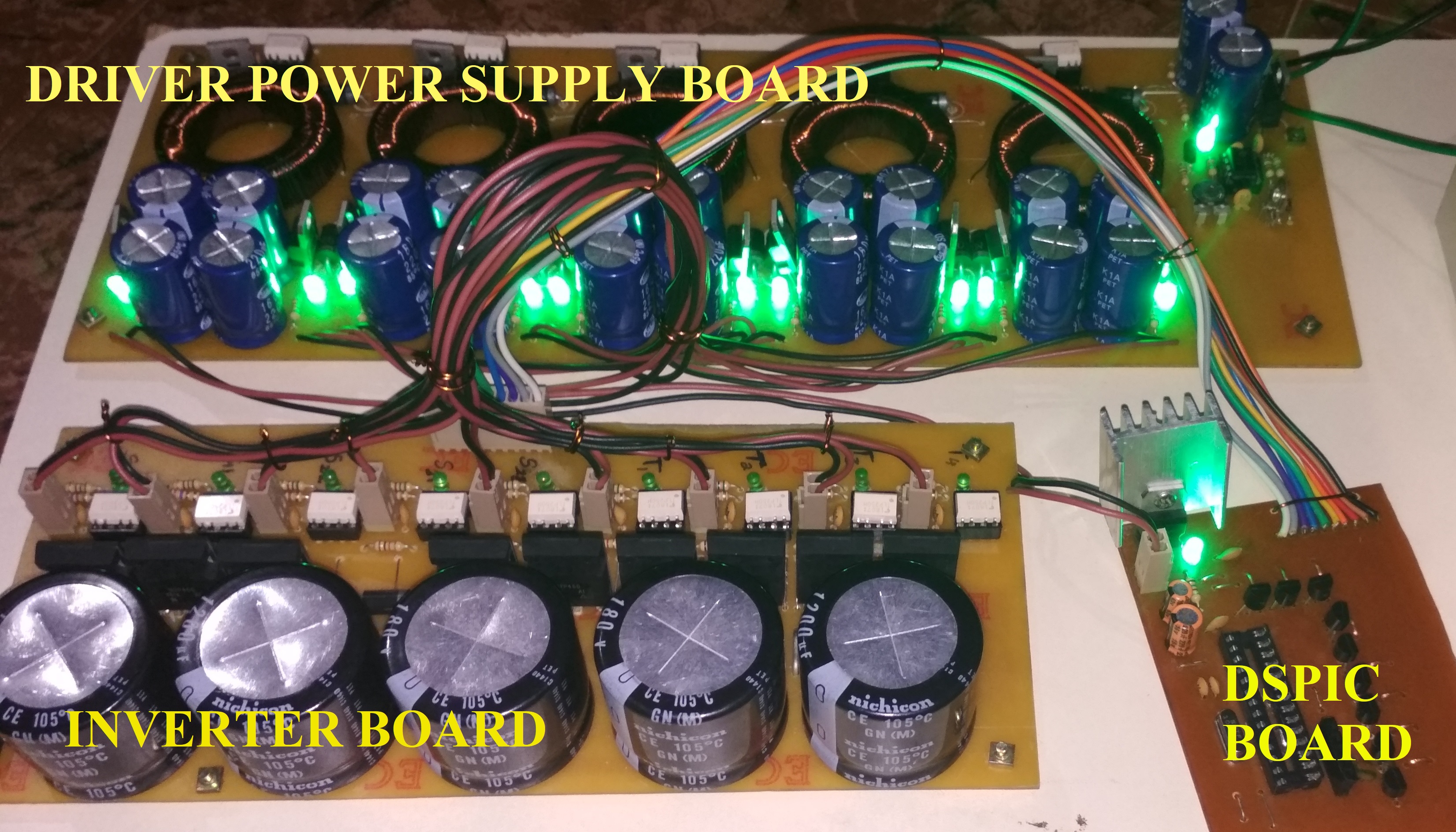
The hardware consists of three integrated circuits:
1. Driver Power Supply Board - Converts 24V input to regulated 15V output
2. Inverter Board - Main power switching circuit with capacitors and diodes
3. DSPIC Control Board - Microcontroller and signal generation
All circuits were etched on copper plates using FeCl₃ displacement method with toner transfer technique.
HARDWARE PERFORMANCE RESULTS
Output Voltage Characteristics
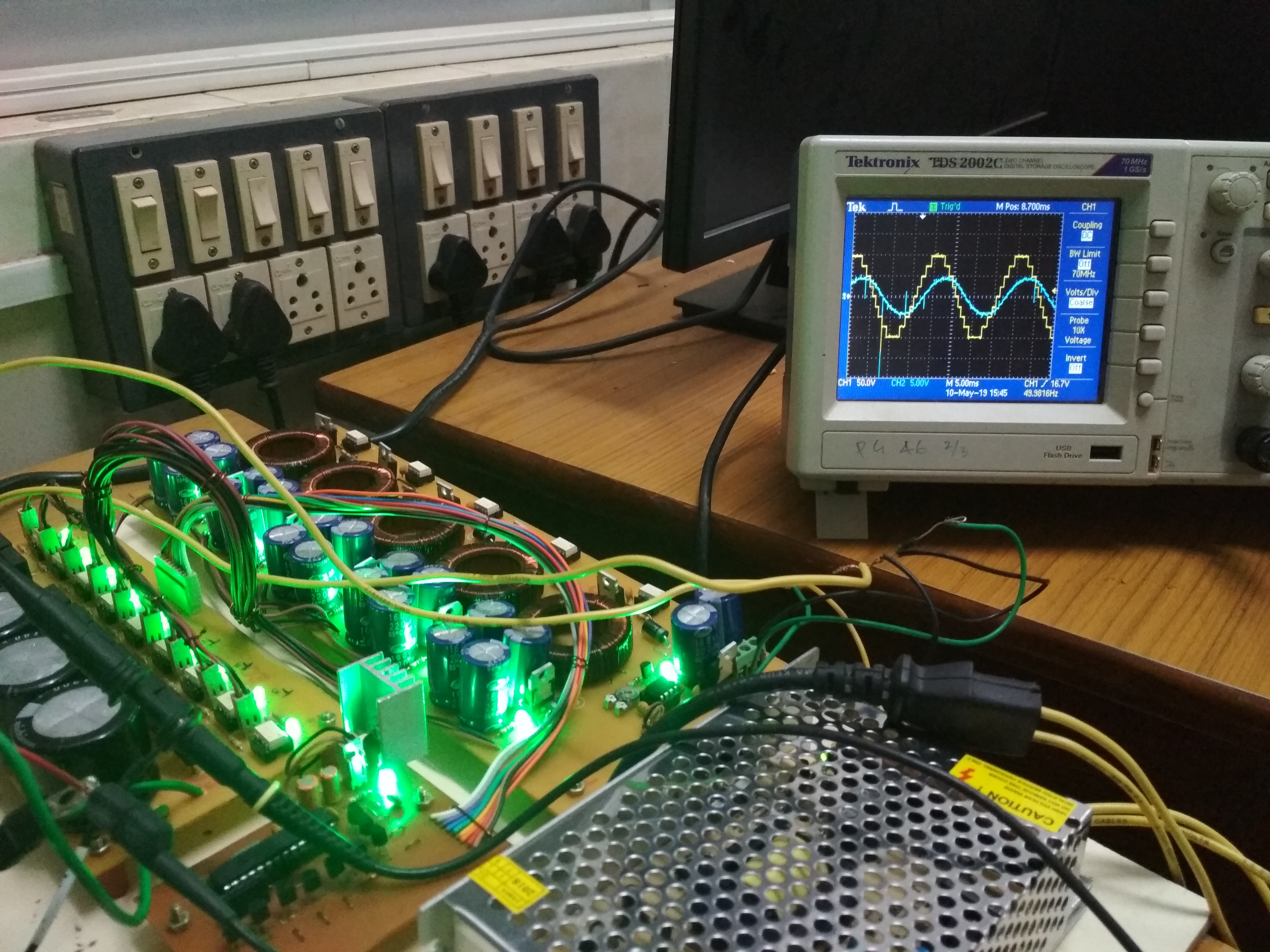
- Peak-to-peak Output: 300 volts
- Voltage Levels: 9 distinct levels observed in output waveform
- Waveform Quality: Smooth stepped waveform with low harmonic content
Testing with Different Loads
- Resistive Load (R = 100Ω): Clean output voltage with minimal current distortion
- RL Load (R = 300Ω, L = 20mH): Output voltage and current waveforms well-filtered at 5 kHz switching frequency
- RL Load (R = 100Ω, L = 40mH): Satisfactory filtering achieved with nine-level switching reducing harmonic content
Key Findings
- Nine-level switching significantly reduces harmonic distortion
- Phase Disposition PWM technique effectively manages switching transitions
- System operates reliably at 5 kHz switching frequency
- Output waveform quality improves with reactive loading
ADVANTAGES OF SWITCHED CAPACITOR TOPOLOGY
- Minimal Component Count - Only 2 capacitors, 2 diodes, and 9 switches for 9-level operation
- Single DC Source - Eliminates need for multiple isolated DC power supplies
- Compact Design - Reduced size due to fewer components
- Cost-Effective - Lower overall system cost compared to traditional MLI topologies
- Simplified Control - Less complex switching strategy reduces control complexity
- Boost Capability - Voltage multiplication achievable without magnetic elements (transformers/inductors)
- Low Harmonic Distortion - Nine-level output reduces THD without heavy filtering
- Scalability - Can be extended to higher voltage levels by adding more SC cells
FUTURE SCOPE
Multilevel inverters present immense potential for next-generation electronic systems:
- High Power Applications - Suitable for medium to high-voltage industrial applications
- Renewable Energy Integration - Potential for solar and wind power conversion systems
- Electric Vehicles - Applications in EV powertrains and charging systems
- Power Quality Improvement - Grid-connected systems with active filtering capabilities
- Three-Phase Systems - Extension to three-phase multilevel inverters
- Advanced Control Techniques - Integration with AI and machine learning for optimized switching
- IoT Integration - Smart monitoring and remote control capabilities
With continued research and development, multilevel inverters based on switched capacitor technology are poised to revolutionize the inverter market in the growing electronics industry.
RELATED DOCUMENTATION
Last Updated: May 15, 2019